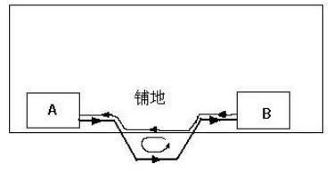
When a PCB board has been laid out and checked for connectivity and spacing without error, is a PCB completed? The answer is of course no. Many beginners also include some experienced engineers. When a PCB board completes the layout and wiring, and checks that the connectivity and spacing are not reported, is a PCB completed? The answer is of course no. Many beginners also include experienced engineers. Due to time constraints or impatience or overconfidence, they often squander things and ignore post-examination. As a result, there are some basic bugs, such as insufficient line width, the component labeling is pressed on the via, the socket is too close, the signal is looped, and so on. As a result, electrical problems or process problems are caused, and serious problems are required to be re-played and waste. Therefore, when a PCB completes the placement and routing, a very important step is the post-check. PCB inspection has many details, and I have listed some of the most basic and most error-prone elements that I consider as post-examination. 1. Component package (1) Pad pitch. If it is a new device, you must draw the component package yourself to ensure proper spacing, and the pad pitch directly affects the soldering of the component. (2) Via size (if any). For plug-in devices, the via size should be sufficient to maintain a sufficient margin, and it is generally appropriate to retain no less than 0.2 mm. (3) Contour silk screen. The outline screen of the device is preferably larger than the actual size to ensure that the device can be installed smoothly. 2, layout (1) IC should not be close to the edge of the board. (2) Devices of the same module circuit should be placed close to each other. For example, the decoupling capacitor should be close to the power supply pin of the IC. The devices that make up the same functional circuit are placed in an area with a clear hierarchy to ensure the realization of the function. (3) Arrange the position of the socket according to the actual installation. The sockets are all lead wires to other modules. According to the actual structure, in order to facilitate the installation, the proximity principle is generally adopted, and the position of the socket is arranged, and generally close to the edge of the board. (4) Pay attention to the direction of the socket. The sockets are all oriented, the direction is reversed, and the wires are re-customized. For flat-plug sockets, the socket orientation should be towards the outside of the board. (5) There must be no devices in the Keep Out area. (6) The source of interference should be kept away from sensitive circuits. High-speed signals, high-speed clocks, or high-current switching signals are all sources of interference and should be kept away from sensitive circuits such as reset circuits and analog circuits. You can use floor covering to separate them. 3, wiring (1) line width size. The line width should be selected in combination with the process and current carrying capacity. The minimum line width cannot be less than the minimum line width of the PCB manufacturer. At the same time, the current carrying capacity is guaranteed, and the appropriate line width is generally selected at 1 mm/A. (2) Differential signal line. For differential lines such as USB and Ethernet, note that the traces should be of equal length, parallel, and plane, and the spacing is determined by the impedance. (3) Pay attention to the return path of the high-speed line. The high-speed line is prone to electromagnetic radiation. If the area of ​​the trace path and the return path is too large, a single-turn coil will form a radiated electromagnetic interference. Therefore, when routing the line, pay attention to the return path. The multi-layer board is provided with a power supply. Layers and ground planes can effectively solve this problem. (4) Pay attention to the analog signal line. The analog signal line should be separated from the digital signal. The trace should be avoided as far as possible from the interference source (such as clock, DC-DC power supply), and the shorter the trace, the better. Medical Caster(Ladle Cover) Medical Caster(Ladle Cover) Medical Caster(Ladle Cover) Ningbo Mywin Caster Co., Ltd. , https://www.mywin-caster.com
4. EMC and signal integrity (1) Termination resistors. A high-speed line or a digital signal line with a high frequency and a long trace is preferably connected to a matching resistor at the end. (2) Connect the signal line and connect a small capacitor. The signal line input from the interface is preferably connected to a small capacitor at a level close to the interface. The size of the capacitor is determined by the strength and frequency of the signal and cannot be too large, otherwise it will affect the signal integrity. For low-speed input signals, such as key inputs, a small 330pF capacitor can be used. (3) Drive capability. For example, a switch signal with a large drive current can be driven by a triode; for a bus with a large number of fanouts, a buffer (such as a 74LS224) can be used. 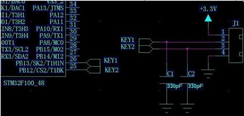
5, silk screen (1) board name, time, PN code. (2) Marking. Label the pins or key signals of some interfaces (such as arrays). (3) Component number. The component numbers should be placed in the appropriate positions, and the dense component numbers can be placed in groups. Be careful not to place it in the hole. 6, other Mark points. For PCBs that require machine soldering, two or three Mark points need to be added. Http://?itemid=438 http://news.chinawj.com.cn 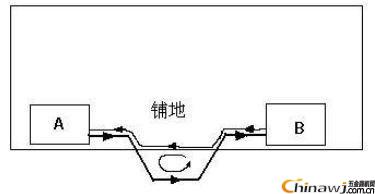 Editor: (Hardware Business Network Information Center) http://news.chinawj.com.cn